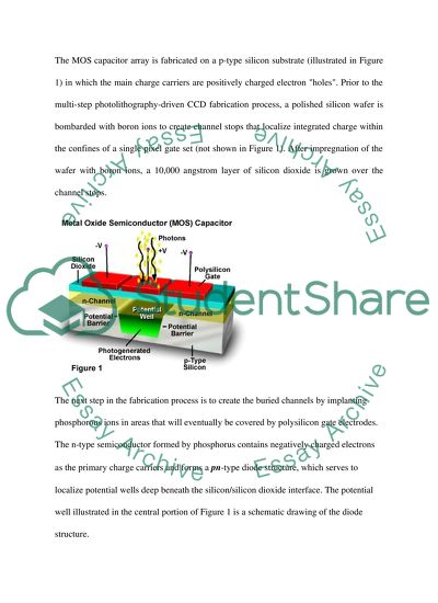
StudentShare
Contact Us
Sign In / Sign Up for FREE
Search
Go to advanced search...
Free

Fabrication of and Characteristics of Silicon Wafer - Essay Example

Cite this document
Summary
The “Fabrication of and Characteristics of Silicon Wafer” paper discusses one of the widely used semiconductor materials found abundantly in nature. Silicon conducts electricity depending on the dopants like boron, phosphorous, arsenic, antimony, etc which are placed into its crystal structure. …
Download full paper File format: .doc, available for editing
GRAB THE BEST PAPER92.5% of users find it useful
Fabrication of and Characteristics of Silicon Wafer
Read Text Preview

Extract of sample "Fabrication of and Characteristics of Silicon Wafer"

The next step in the fabrication process is to create the buried channels by implanting phosphorous ions in areas that will eventually be covered by polysilicon gate electrodes. The n-type semiconductor formed by phosphorus contains negatively charged electrons as the primary charge carriers and forms a type diode structure, which serves to localize potential wells deep beneath the silicon/silicon dioxide interface. The potential well illustrated in the central portion of Figure 1 is a schematic drawing of the diode structure.

The primary function of the buried channel is to localize integrated electrons away from the silicon/silicon dioxide interface, where they can become trapped during charge transfer. By localizing charge deep within the p-type silicon substrate, transfer of charge occurs more efficiently with a minimum of residual charge remaining in the gate. After the buried channels are formed within the silicon substrate, a layer of silicon dioxide is thermally grown on the silicon wafer surface to provide an insulating base for the gate electrodes.

Next, a phosphorus-doped layer of polycrystalline silicon (polysilicon) about 5,000 angstroms thick is grown on top of the oxide layer. This layer of polysilicon comprises the gate electrodes (see Figure 1) and is transparent to visible light, making it an ideal substance for use in CCDs. Although the fabrication of a complete CCD takes additional steps, the basics of the MOS capacitor assembly have been completed at this point."I Vs V Characteristics(According to M.Aceves, O.Malik, V. Grimalsky V.5 No. 2 (2004) P. 236-237), National Institute for Astrophysics, Optics, and Electronics ( INAOE), Electronics Department.)The dynamic I-V characteristics of these MOS structures when a linear voltage sweep (60 v/ sec) was applied to the metallic semitransparent gate are shown in the diagrams below.

Dynamic I-V Characteristics of fabricated MOS capacitor with silicon dioxide as insulator with positive (above) and negative (below) charge recorded when a triangular sweep voltage ( 60 v/s) was applied to the gate. 

Read More
Cite this document
  • APA
  • MLA
  • CHICAGO
(Silicon Wafer Essay Example | Topics and Well Written Essays - 500 words, n.d.)
Silicon Wafer Essay Example | Topics and Well Written Essays - 500 words. Retrieved from https://studentshare.org/engineering-and-construction/1503428-clean-room-assignment-engineering-practice
(Silicon Wafer Essay Example | Topics and Well Written Essays - 500 Words)
Silicon Wafer Essay Example | Topics and Well Written Essays - 500 Words. https://studentshare.org/engineering-and-construction/1503428-clean-room-assignment-engineering-practice.
“Silicon Wafer Essay Example | Topics and Well Written Essays - 500 Words”. https://studentshare.org/engineering-and-construction/1503428-clean-room-assignment-engineering-practice.
  • Cited: 0 times

CHECK THESE SAMPLES OF Fabrication of and Characteristics of Silicon Wafer

High Density Plasma Chemical Vapor Deposition

While doing the edge gap filling some factors are also keep in consideration like raising the wafer temperature, plasma density and lowering of the deposition pressure.... These include silicon, carbon, nitrites, carbides, oxides and also many others.... In the semiconductor world, CVT is majorly used in the fabrication process of the semiconductor devices and to the exposure of the amorphous SiO2, silicon Germanium, and tungsten, etc.... The high-density plasma is generated by the gases including oxygen, silicon, hydrogen, and a chemical etching gas which is nitrogen free....
8 Pages (2000 words) Assignment

VLSI Technology and Reliability

In recent world, SOI fabricators continue to be researched on due to their use in fabrication of the CMOS's ICs (Marshall and Natarajan, 2002).... Some of these methods are the SOI-wafer, p-wafer and n-wafer.... Modern usage of SOI wafer 1.... SOI (silicon on Insulator) well fabricator on CMOS It was used in selected discrete and integrated circuits in 1960s.... These devices were fabricated with SOS (silicon on sapphire), but recently they are fabricated with SIMOX (separation by Implanted Oxygen)....
5 Pages (1250 words) Essay

Pick a Chemical Industry or Book Chapter

The majority of silicon found in nature is used in steel refining and aluminum casting.... The highly purified form of silicon is used in integrated circuits.... The final commodities of silicon are necessary in the modern world because of our immense dependence on this element.... Portland cement is a crucial and commodity of silicon.... And finally, fiberglass, glass fibers, and optical fibers (including glassful) are the end products of silicon elements that form the backbone in the ceramics industry....
7 Pages (1750 words) Essay

Review Paper

n the fabrication d the design, the InAlAs-InGaAs-lnP lattice matched epitaxial layers were developed by the organo metallic vapor phae epitaxy on the lnP:Fe substrate.... The paper aimed at designing, fabricating and characterizing a high speed and high sensitivity vertical indium-tin-oxide-InAIAs-InGaAs Schottky barrier photo-detector....
7 Pages (1750 words) Research Paper

The Fabrication of the Pentacene Thin Film Transistor

The paper 'The fabrication of the Pentacene Thin Film Transistor' looks at a fused-ring polycyclic aromatic hydrocarbon, presents relatively high carrier mobility when used for fabricating the organic thin-film transistors and this means that pentacene is widely used as the active material.... However, the monocrystalline materials, such as gallium arsenide (GaAs), that showed the greatest promise for fabrication of high-speed TFTs are expensive to source in the required purity and costly to process, rendering manufacturing of large-area devices manufactured using such materials prohibitively expensive (Kagan, 2003, Chapter 6)....
10 Pages (2500 words) Research Proposal

Organic Thin Film Transistor

The fact that the electrical characteristics of the organic TFTs in the linear region do not match the ideal is due to a varying potential drop at the source and drain contacts.... However, the monocrystalline materials, such as gallium arsenide (GaAs), that showed the greatest promise for fabrication of high-speed TFTs are expensive to source in the required purity and costly to process, rendering manufacturing of large-area devices manufactured using such materials prohibitively expensive (Kagan, 2003, Chapter 6)....
12 Pages (3000 words) Case Study

The Different Modes of Fabrication in CMOS

This fabrication of CMOS was developed in the 1980s.... In the recent world, SOI fabricators continue to be researched due to their use in the fabrication of the CMOS's ICs (Marshall and Natarajan, 2002).... These devices were fabricated with SOS (silicon on sapphire), but recently they are fabricated with SIMOX (separation by Implanted Oxygen).... It starts with a moderately doped p_type silicon substrate.... The paper "The Different Modes of fabrication in CMOS" presents CMOS that is getting to look as if it is like an irreplaceable technology shortly due to its many uses....
5 Pages (1250 words) Essay

Construction Material Project

The major characteristics of fly ash that make it the preferred material for this project is that it has a low calcium oxide content (<10%) and is classified as pozzolanic and hence will be used as part of the binder content in a concrete mix.... The report "Construction Material Project" focuses on the critical analysis of the design concept that incorporates concrete mix design, the selection of steel to be used, and the specifications for both concrete and steel preferred for the intended project....
7 Pages (1750 words) Report
sponsored ads
We use cookies to create the best experience for you. Keep on browsing if you are OK with that, or find out how to manage cookies.
Contact Us