StudentShare
Contact Us
Sign In / Sign Up for FREE
Search
Go to advanced search...
Free

Basic Elements and Attributes that Relate to Logic Circuits - Coursework Example

Cite this document
Summary
"Basic Elements and Attributes that Relate to Logic Circuits" paper offers an insightful introduction regarding logic circuits featuring a detailed description of logic circuits and then proceeds to outline various electrical and electronic issues that relate to their design and implementation…
Download full paper File format: .doc, available for editing
GRAB THE BEST PAPER92.9% of users find it useful
Basic Elements and Attributes that Relate to Logic Circuits
Read Text Preview

Extract of sample "Basic Elements and Attributes that Relate to Logic Circuits"

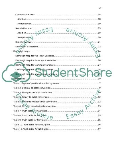
Contents Executive summary 5 Introduction 5 Types of logic circuits 6 Numbering systems and conversion 6 Positional number system 6 Decimal numbers 8Binary system 8 Octal number system 8 Hexadecimal number system 8 Numbering Conversions 9 Decimal number system conversion 9 Decimal fraction conversion 10 Binary conversion 11 Octal to hexadecimal conversion 12 Logic gates 13 Basic logic gates 13 AND gate 13 OR gate 14 NOT gate 15 Combinational logic gates 16 NAND gate 16 NOR gate 16 Exclusive- OR (EXOR) gate 17 Boolean algebra 18 Commutative laws 18 Addition 18 Multiplication 19 Associative laws 19 Addition 19 Multiplication 20 Distributive law 21 Demorgan’s theorems 22 Karnaugh maps 24 Karnaugh map for two input variables 25 Karnaugh map for three input variables 26 Karnaugh map for four input variables 27 Karnaugh map for six-input variables 28 Karnaugh map for seven-input variables 29 References 30 Table 1. Types of positional number systems 7 Table 2. Decimal to octal conversion 9 Table 3. Binary to decimal conversion 10 Table 4. Binary to octal conversion 11 Table 5. Binary to hexadecimal conversion 12 Table 6. Octal to hexadecimal conversion 13 Table 7. Truth table for AND gate 14 Table 8. Truth table for OR gate 15 Table 9. Truth table for NOT gate 15 Table 10. Truth table for NAND gate 16 Table 11. Truth table for NOR gate 17 Table 12. Truth table for EXOR gate 17 Table 13. Basic rules of Boolean algebra 21 Table 14. Truth table for Demorgan’s first theorem 23 Table 15. Truth table for Demorgan’s second theorem 24 Table 16. Truth table for logical expressions with two inputs 25 Table 17. Truth table for logical expressions with three inputs 26 Figure 1. A simple logic circuit. This figure illustrates a logic circuit consisting of three logic gates (AND, OR and NOT gates). 6 Figure 2. An AND gate. The figure illustrates an AND operation in an AND gate. 14 Figure 3. An OR gate. The figure illustrates an OR operation in an OR gate. 14 Figure 4. A NOT gate. The figure illustrates a NOT operation in an inverter. 15 Figure 5. A NAND gate. The figure illustrates the combination of a NOT gate with an AND gate to form a NAND gate. 16 Figure 6. A NOR gate. The figure illustrates the combination of a NOT gate with an OR gate to form a NOR gate. 17 Figure 7. An EXOR gate. The figure illustrates the operation of an EXOR gate. 17 Figure 8. The commutative law of addition. The figure illustrates sum equivalence as stated by the commutative law of addition. 18 Figure 9. The commutative law of multiplication. The figure illustrates product equivalence as stated by the commutative law of multiplication. 19 Figure 10. The associative law of addition. The figure illustrates sum equivalence as stated by the associative law of addition. 20 Figure 11. The associative law of multiplication. The figure illustrates product equivalence as stated by the associative law of multiplication. 20 Figure 12. The distributive law. The figure illustrates sum and product equivalence as stated by the distributive law. 21 Figure 13. Demorgan’s first theorem. The figure illustrates the equivalence between the complement of a product and the sum of complements as stated by Demorgan’s first theorem. 23 Figure 14. Demorgan’s second theorem. The figure illustrates the equivalence between the complement of a sum and the product of complements as stated by Demorgan’s second theorem. 24 Figure 15. Karnaugh map for two-input variables. The figure illustrates the simplification of two-input-variable logical expressions using Karnaugh maps. 25 Figure 16. Karnaugh map for three-input variables. The figure illustrates the simplification of three-input-variable logical expressions using Karnaugh maps. 27 Figure 17. Karnaugh map for four-input variables. The figure illustrates the simplification of four- input-variable logical expressions using Karnaugh maps. 27 Figure 18. Karnaugh map for six-input variables. The figure illustrates the simplification of six-input-variable logical expressions using Karnaugh maps. 29 Figure 19. Karnaugh map for seven-input variables. The figure illustrates the simplification of seven-input-variable logical expressions using Karnaugh maps. 30 Logic Circuits Executive summary The following report presents a comprehensive evaluation of the basic elements and attributers that relate to logic circuits. The report offers an insightful introduction regarding logic circuits featuring a detailed description of logic circuits and then proceeds to outline various electrical and electronic issues that relate to their design and implementation. The body of the report begins with an in-depth discussion on number systems in order to shed light on the binary system; which is the dominant computer number system. The next section discusses logic gates starting with the three most basic gates followed by combinational logic gates. The report contains illustrations and truth tables ensuring a vivid illustration on the application of logic gates in logic circuits and their relationship with logic operations. The report also discusses Boolean algebra, an integral field in the study of logic circuits, and the laws and rules that govern the creation and simplification of logical expressions. The report concludes with an invaluable lesson, albeit introductory, on the application of Karnaugh maps in the simplification of multivariable logical expressions and a brief reflection on the popularity of digital systems. Introduction The advent of digital systems has led to the design of logic circuits which variably represents digital logic as defined by various Boolean expressions. According to Rafiquzzaman and Chandra (1988), a logic circuit is a directed acyclic graph which computes a binary function mapping the values of its output from the values of its input variables. Logic circuits contain gates and transmission wires which carry input digital signals and emit a single output digital signal (see Figure 1 below). Several digital features characterize the design of logic circuits, these include; Boolean expressions and algebra, logic gates, and the simplification or enhancement of the logic circuit using various logic techniques such as Karnaugh maps. Figure 1. A simple logic circuit. This figure illustrates a logic circuit consisting of three logic gates (AND, OR and NOT gates). Types of logic circuits There are several logic circuit classes with the most popular classes being the transistor-transistor logic (TTL), and complementary symmetry metal-oxide-semiconductor (CMOS); popular because they have several functional and operational advantages. Numbering systems and conversion A number system represents quantity by defining a set of values for example, the number of students in a class. There are two categories of number systems; non-positional and positional number systems. Positional number system The most common positional number system is the decimal number system; others include the binary number system, the octal number system and the hexadecimal number system (Latif, Ullah and Jan, 2011). Table 1 below illustrates the different positional number systems and their representative numbers and characters. Table 1. Types of positional number systems Decimal Binary Octal Hexadecimal 0 0000 0 0 1 0001 1 1 2 0010 2 2 3 0011 3 3 4 0100 4 4 5 0101 5 5 6 0110 6 6 7 0111 7 7 8 1000 10 8 9 1001 11 9 10 1010 12 A 11 1011 13 B 12 1100 14 C 13 1101 15 D 14 1110 16 E 15 1111 17 F Decimal numbers The decimal number system is the most commonly used system by humans and it consists of ten digits from zero to nine which are referred to as the symbols of the decimal system (Latif, Ullah and Jan, 2011). The decimal number system presents digits in a base ten number meaning that each digit represents a value or units ten times the number to its right. For example: 6752= 6000+700+50+2= (6 x 10 3) + (7 x 10 2) + (5 x 10 1) + (2 x 10 0) Binary system Computer systems are always in two operational states, which are, on or off and hence the computer uses two numbers i.e. 1 and 0 (Latif, Ullah and Jan, 2011). One represents an on state and zero represents an off state and these two numbers are the only digits in a binary system; a binary system is in a base two meaning that the nth bit on the right hand side is nth bit x 2 n-1. Octal number system The octal numbers system is similar to the binary and decimal number system except that it has eight digits, zero to seven in a base eight (Latif, Ullah and Jan, 2011). This number system uses a power of eight to determine the digit of a number’s position in its presentation. Hexadecimal number system This number system is similar to the others except that the digits are in a base sixteen meaning that each digit in the system represents a power of the sixteen. The system uses ten numbers, zero to nine to represent their equivalent and six characters, A to F to represent ten to fifteen respectively (Latif, Ullah and Jan, 2011). Numbering Conversions There are many methods that are sued to convert any number in one system to another number system and it is important to note that any number can be converted into all the other number systems. Decimal number system conversion Decimal numbers are converted to their radix equivalents through successive division using the base radix of the target number system (Latif, Ullah and Jan, 2011). This means that; for binary numbers divide by two, octal numbers divide by eight and hexadecimal numbers divide by 16. You must divide the number until the quotient is zero noting the remainder in each case at the right hand side. After the quotient is zero, write the remainders in reverse order to get the number for any number system according to the radix divisor (see Table 2). An example of decimal to octal conversion- Convert (85)10 into octal number: Table 2. Decimal to octal conversion Base/Radix Quotient Remainder 8 85 5 8 10 2 8 1 1 0 Reverse the remainder to get Octal equivalent = (125)8 Converting any number system to decimal equivalent Write the weight of each digit in the number and then get the weighted value by multiplying the weighted position with the respective bit and then add the weighted values to get the decimal number (see Table 3). For example-Convert the binary number (101100)2 into decimal number: Table 3. Binary to decimal conversion Binary Number Weight of each bit Weighted Value Computed value 1 25 1 x 25 32 0 24 0 x 24 0 1 23 1 x 23 8 1 22 1 x 22 4 0 21 0 x 21 0 0 20 0 x 20 0 Decimal number 44 Decimal fraction conversion In order to convert any decimal fraction to any other number system, multiply successively with the radix of the target number system (Latif, Ullah and Jan, 2011). You must multiply the decimal fraction with the radix and note then evaluate the result, if a non-zero integer is generated, record the integer. You must then remove the integer and multiply the fraction again until the value of the fraction becomes zero. Finally, you write the recorded integers in order of occurrence to get the converted equivalent. For example-Convert (0.85)10 into hexadecimal number: 0.852 x 16 = 13.6; record 13 or D and continue multiplying the fraction 0.6 x 16 =9.6; record 9 and continue 0.6 x 16 = 9.6; record nine and continue 0.6 x 16 = 9.6; record nine and approximate to four decimal places The hexadecimal equivalent = (0.D999)16 Binary conversion Binary to octal conversion Because the radix for the octal number system is the third power of the radix for binary numbers (23=8), we convert binary numbers to octal numbers by first grouping the binary number into groups of three digits from the left to the right and then converting each group into its octal equivalent (see Table 4). It is important to note that for octal to binary conversion, you reverse the process, i.e. convert each octal digit to its binary equivalent (Latif, Ullah and Jan, 2011). For example, convert (111101101)2 to octal number Table 4. Binary to octal conversion Binary groups of three Octal equivalent 111 7 101 5 101 5 The octal equivalent = (755)8 Binary to hexadecimal Follow the process for binary to octal but group the binary number into groups of four because; (24=16); and you should reverse the process to get a binary number from a hexadecimal number (see Table 5). For example, convert (11101100)2 to hexadecimal number Table 5. Binary to hexadecimal conversion Binary groups of four Hexadecimal equivalent 1100 C 1110 E CE Octal to hexadecimal conversion Convert the number to its binary equivalent and then convert to hexadecimal equivalent (see Table 6). It is important to note that for hexadecimal to octal conversion, convert the hexadecimal number to binary equivalent and then convert to octal equivalent (Latif, Ullah and Jan, 2011). For example-Convert (45)8 into hexadecimal number: 85 to binary= 100101 Change to hexadecimal Table 6. Octal to hexadecimal conversion Binary groups of four Hexadecimal equivalent 0101 5 0010 2 52 Logic gates Logic circuits are electrical circuits which are implemented from logical expressions and the logic expressions are defined by logic operations involving Boolean variables. Marcovitz (2005) states that there are three basic logic operations namely; OR operation, AND operation, and NOT operation. Logic gates are electronic devices which make logical decisions based on these logical operations and they are also called switches (Marcovitz, 2005). Logic gates are described in truth tables which contain rows for very possible combination of inputs values in a logic circuit indicating the output values for each combination of input values. Basic logic gates AND gate This is an electronic circuit that gives a true output or one only if all the inputs are true (see Table 7) (Marcovitz, 2005). The AND gate denotes an AND operation and the operation is sometimes illustrated with a dot; A.B or simply AB (see Figure 2). Figure 2. An AND gate. The figure illustrates an AND operation in an AND gate. Table 7. Truth table for AND gate A (input) B (input) C (output) 0 0 0 0 1 0 1 0 0 1 1 1 OR gate This is an electronic circuit that gives a true output if one or more of the inputs are true (see Table 8). The OR gate denotes an OR operation which is usually indicated with plus sign, A + B (see Figure 3). Figure 3. An OR gate. The figure illustrates an OR operation in an OR gate. Table 8. Truth table for OR gate A (input) B (input) C (output) 0 0 0 0 1 1 1 0 1 1 1 1 NOT gate This is an electronic circuit that produces an inverted value of its input as the output (see Table 9). It is also referred to as an inverter and it denotes the NOT operation (see Figure 4). Figure 4. A NOT gate. The figure illustrates a NOT operation in an inverter. Table 9. Truth table for NOT gate A (input) C (output) 0 1 1 0 Combinational logic gates NAND gate This is a combinational logic gate which is created by combining a NOT with an AND gate, i.e. an AND gate followed by a NOT gate (see Figure 5). The outputs of all NAND gates are true if any of the inputs are false (see Table 10). Figure 5. A NAND gate. The figure illustrates the combination of a NOT gate with an AND gate to form a NAND gate. Table 10. Truth table for NAND gate A (input) B (input) C (output) 0 0 1 0 1 1 1 0 1 1 1 0 NOR gate This is a combinational logic gate which is created by combining a NOT with an OR gate, i.e. an OR gate followed by a NOT gate (see Figure 6). The outputs of all NOR gates are false if any of the inputs are true (see Table 11). Figure 6. A NOR gate. The figure illustrates the combination of a NOT gate with an OR gate to form a NOR gate. Table 11. Truth table for NOR gate A (input) B (input) C (output) 0 0 1 0 1 0 1 0 0 1 1 0 Exclusive- OR (EXOR) gate This is a combinational logic gate which gives a true output if either, but not both, of its inputs are true (see Figure 7 and Table 12). An Exclusive-NOR (EXNOR) gate is the opposite of EXOR i.e. it gives false outputs is either, but not both, of its inputs are true (Marcovitz, 2005). Figure 7. An EXOR gate. The figure illustrates the operation of an EXOR gate. Table 12. Truth table for EXOR gate A (input) B (input) C (output) 0 0 0 0 1 1 1 0 1 1 1 0 Boolean algebra Boolean algebra implements the basic laws that apply in ordinary algebra and consists of three basic laws; commutative and associative laws for addition and multiplication, and the distributive law. Commutative laws Addition The commutative law of addition states that the order of addition or ORing does not make any difference (see Figure 8; note that denotes equivalence) (Marcovitz, 2005). Illustration: A + B = B + A Figure 8. The commutative law of addition. The figure illustrates sum equivalence as stated by the commutative law of addition. Multiplication The commutative law of addition states that the order of multiplication or ANDing does not make any difference (see Figure 9; note that denotes equivalence) Illustration: A.B = B.A Figure 9. The commutative law of multiplication. The figure illustrates product equivalence as stated by the commutative law of multiplication. Associative laws Addition The associative law of addition states that the grouping of variables does not make any difference when adding or ORing more than two variables (see Figure 10; note that denotes equivalence) (Marcovitz, 2005). Illustration:A + (B + C) = (A +B)+C Figure 10. The associative law of addition. The figure illustrates sum equivalence as stated by the associative law of addition. Multiplication The associative law of multiplication states that the grouping of variables does not make any difference when multiplying or ANDing more than two variables (see Figure 11; note that denotes equivalence). Illustration: A (BC) = (AB) C Figure 11. The associative law of multiplication. The figure illustrates product equivalence as stated by the associative law of multiplication. Distributive law The distributive law states that ORing or adding two or more variables and then multiplying or ANDing the sum with a single variable is equivalent to multiplying or ANDing the single variable with each of the two or more variables and then adding or ORing the products (see Figure 12; note that denotes equivalence) (Rafiquzzaman and Chandra, 1988). Illustration: A (B + C) = AB + AC Figure 12. The distributive law. The figure illustrates sum and product equivalence as stated by the distributive law. According to Marcovitz (2005), this law also defines the factoring process where you can factor out a common variable from the product terms (see Table 13). That is: AB + AC = A (B + C) Table 13. Basic rules of Boolean algebra 1 A + 0 = A 2 A + 1 = 1 3 A. 0 = 0 4 A. 1 = A 5 A + A = A 6 A + = 1 7 A. A = A 8 A. = 0 9 = A 10 A + AB = A 11 A + AB = A+ B 12 (A + B)(A + C) = A + BC Note. (A,B, or C can represent one variable or group of variables) Demorgan’s theorems The first theorem states that the complement of a product is equal to the sum of the complements of the variables (see Table 14) (Rafiquzzaman and Chandra, 1988). This means that the complement of two or more ANDed variables is equivalent to the OR of the complements of the individual variables (see Figure 13; note that denotes equivalence). = + Figure 13. Demorgan’s first theorem. The figure illustrates the equivalence between the complement of a product and the sum of complements as stated by Demorgan’s first theorem. Table 14. Truth table for Demorgan’s first theorem INPUTS OUTPUTS X Y + 0 0 1 1 0 1 1 1 1 0 1 1 1 1 0 0 The second theorem states that the complement of a sum of variables is equal to the product of the complements of the variables (see Table 15). This means that the complement of two or more ORed variables is equivalent to the AND of the complements of the individual variables (see Figure 14; note that denotes equivalence) (Rafiquzzaman and Chandra, 1988). = Figure 14. Demorgan’s second theorem. The figure illustrates the equivalence between the complement of a sum and the product of complements as stated by Demorgan’s second theorem. Table 15. Truth table for Demorgan’s second theorem INPUTS OUTPUTS X Y 0 0 1 1 0 1 0 0 1 0 0 0 1 1 0 0 Karnaugh maps Karnaugh maps refer to a method that is relatively easy to implement when minimizing Boolean expressions in multivariable logic circuits (Rizzoni and Hartley, 2000). Karnaugh maps group together expressions with common factors thereby eliminating unwanted variables and presenting a vivid pictorial logical model. Karnaugh maps are created from truth tables and the output values are presented inside the squares meaning that there is one square in the map for every row in the truth table and the edges represent the input values of the input variables (Rizzoni and Hartley, 2000). Karnaugh maps also allow combination of two or more adjacent squares using looping to further simplify the equation. Karnaugh map for two input variables Consider the following truth table: Table 16. Truth table for logical expressions with two inputs A B X 0 0 0 0 1 1 1 0 0 1 1 1 The logical expression for this truth table is: X = A. B +. B (see Table 16). The Karnaugh map for this logical expression is shown below: A B 1 1 0 0 Figure 15. Karnaugh map for two-input variables. The figure illustrates the simplification of two-input-variable logical expressions using Karnaugh maps. Considering the map above, the two adjacent one’s (highlighted) are grouped together and one can see that A has both states (true and false) in the group. This eliminates variable A; and the remaining variable B which has the true state in both squares is picked as the simplified form, i.e. X = B (see Figure 15 above). Karnaugh map for three input variables Consider the following truth table: Table 17. Truth table for logical expressions with three inputs A B C X 0 0 0 1 0 0 1 1 0 1 0 1 0 1 1 0 1 0 0 0 1 0 1 0 1 1 0 1 1 1 1 0 The Boolean expression for this truth table is: X =.. + ..C + .B. + A.B. (see Table 17). The Karnaugh map for this logical expression is shown below: AB A B C 0 0 1 0 1 0 1 1 Figure 16. Karnaugh map for three-input variables. The figure illustrates the simplification of three-input-variable logical expressions using Karnaugh maps. After combining two adjacent squares, the simplified expression is: X =. + B. (see Figure 16 above). Karnaugh map for four input variables Consider the Boolean expression below: X =... D +..C. D +. B. . D + .B.C.D The Karnaugh map for this logical expression is shown below: AB A B CD 0 0 1 1 C 0 0 0 0 0 0 0 0 D 0 0 1 1 Figure 17. Karnaugh map for four-input variables. The figure illustrates the simplification of four- input-variable logical expressions using Karnaugh maps. As illustrated in the Karnaugh map, we can combine four adjacent squares meaning that the simplified expression will consist of two variables only. The adjacent squares in the row eliminate variable B, while the adjacent squares in the column eliminate variable C and the simplified expression is: X = A.D (see Figure 17 above). Karnaugh map for six-input variables A six-variable Karnaugh map is treated as four layers of sixteen cells each. It is important to note that cells situated directly above and below each other are adjacent. Consider the Boolean expression below: X =...D.E . +..C. D .F +..C. .F + ..C.D.E . + .B.C.D. .F +.B.C.. .F +A.... . +A....E . +A...D.E . +A..C.D.E . The Karnaugh map for this logical expression is shown below: EF AB=00 CD AB=O1 CD AB=11 CD AB=10 CD 00 01 11 10 00 01 11 10 00 01 11 10 00 01 11 10 00 0 0 0 0 0 0 0 0 0 0 0 0 1 0 0 0 01 0 0 1 1 0 0 1 1 0 0 0 0 0 0 0 0 11 0 0 0 0 0 0 0 0 0 0 0 0 0 0 0 0 10 0 1 1 0 0 0 0 0 0 0 0 0 1 1 1 0 Figure 18. Karnaugh map for six-input variables. The figure illustrates the simplification of six-input-variable logical expressions using Karnaugh maps. As illustrated in the Karnaugh map, we can apply cell adjacency on the squares that are similarly colored. After applying the elimination rules discussed above the resultant simplified expression is: X=. C .F +.D.E. +A...(see Figure 18 above). Karnaugh map for seven-input variables A seven-variable Karnaugh map is treated as four layers of thirty two cells each. It is important to note that cells situated directly above and below each other are adjacent. Consider the Boolean expression below: X =A..C. D..F.G + A..C. D.E.F.G + A.B.C..E ..G + A.B.C..E .F.G + A.B.C.D. .. + A.B.C.D. ..G + A.B.C.D. .F. + A.B.C.D.E .. + A.B.C.D.E..G + A.B.C.D.E.F. X BC=00 FG BC=O1 FG BC=10 FG BC=11 FG 00 01 11 10 00 01 11 10 00 01 11 10 00 01 11 10 ADE 000 0 0 0 0 0 0 0 0 0 0 0 0 0 0 0 0 001 0 0 0 0 0 0 0 0 0 0 0 0 0 0 0 0 011 0 0 0 0 0 0 0 0 0 0 0 0 0 0 0 0 010 0 0 0 0 0 0 0 0 0 0 0 0 0 0 0 0 DE 100 0 0 0 0 0 0 0 0 0 0 0 0 0 0 0 0 101 0 0 0 0 0 0 0 0 0 0 0 0 0 1 1 0 111 0 0 0 0 0 0 1 0 0 0 0 0 1 1 0 1 110 0 0 0 0 0 0 1 0 0 0 0 0 1 1 0 1 Figure 19. Karnaugh map for seven-input variables. The figure illustrates the simplification of seven-input-variable logical expressions using Karnaugh maps. As illustrated in the Karnaugh map, we can apply cell adjacency on the squares that are similarly colored. After applying the elimination rules discussed above the resultant simplified expression is: X=A..C.D.F.G + A.B.C.D . + A.B.C.D.F. + A.B.C..E.G (see Figure 19 above). References Abdelilah, A., 1989. Truth tables, minterms, maxterms, Karnaugh maps. Chesterfield, Ohio:Weber Systems, Inc. Hambley, A. R., Kumar, N. and Kulkarni, A. R., 2008. Electrical engineering: principles and applications. Pearson Prentice Hall. Langholz, G., Kandel, A. and Mott, J. L., 1988. Digital logic design. Dubuque, Iowa: Wm. C. Brown. Latif, S., Ullah, R. and Jan, H., 2011. A Step towards an Easy Interconversion of Various Number Systems. [pdf] arXiv preprint arXiv:1107.1663. Available at: [Accessed 19 September 2014]. Marcovitz, A. B., 2005. Introduction to logic design. Boston, McGraw-Hill Higher Education. Nelson, V. P., Nagle, H. T. and Irwin, J. D., 1995. Digital logic circuit analysis. New Jersey, USA: Prentice-Hall International Inc. Rafiquzzaman, M. and Chandra, R., 1988. Modern computer architecture. St. Paul: West Pub. Co. Rizzoni, G. and Hartley, T. T., 2000. Principles and applications of electrical engineering (Vol. 3). McGraw Hill. Read More
Cite this document
  • APA
  • MLA
  • CHICAGO
(Basic Elements and Attributes that Relate to Logic Circuits Coursework Example | Topics and Well Written Essays - 4500 words, n.d.)
Basic Elements and Attributes that Relate to Logic Circuits Coursework Example | Topics and Well Written Essays - 4500 words. https://studentshare.org/engineering-and-construction/1839308-report
(Basic Elements and Attributes That Relate to Logic Circuits Coursework Example | Topics and Well Written Essays - 4500 Words)
Basic Elements and Attributes That Relate to Logic Circuits Coursework Example | Topics and Well Written Essays - 4500 Words. https://studentshare.org/engineering-and-construction/1839308-report.
“Basic Elements and Attributes That Relate to Logic Circuits Coursework Example | Topics and Well Written Essays - 4500 Words”. https://studentshare.org/engineering-and-construction/1839308-report.
  • Cited: 0 times

CHECK THESE SAMPLES OF Basic Elements and Attributes that Relate to Logic Circuits

Capacitance (Timing Circuits)

iming CircuitIn timing circuits there are two possibilities either we are controlling the rate of response of the capacitor or controlling the rate of voltage across the capacitor.... n timing circuits when a capacitor is charged through a resistor then the voltage equation is given byV(t) = V0 * e-t/RC....
2 Pages (500 words) Essay

Common and Basic Attributes Across the Three Sites

he other attributes that were rejected were either irrelevant or less important and could be retrieved through the major attributes such as the auction, seller/buyer, or product ids.... This paper "Common and Basic attributes Across the Three Sites" focuses on the SQL code that outputs data as predicted; the product id, Seller id, starting bid closing bid payment details shipping id, and payment methods are displayed form both the auction and payment tables as predicted....
8 Pages (2000 words) Assignment

Packet Switching vs. Circuit Switching

Packets are handled either through the virtual circuits or through the data gram.... Circuit switching technique was predominately used for the purpose of transmitting signals and streams across the network.... Circuit switch… nique has been in use since long, ever since the times when the simple telephone sets were in practice and there was no concept of digital transmission nor bits, and packet switch was predominately introduced as soon as the digital interface of transmission became common. While Packet switched vs....
2 Pages (500 words) Assignment

DC Circuit Basics

A parallel-plate capacitor holds 10 μC of charge on each plate when connected to a 12 V battery.... If you were to slide a dielectric between the plates while the battery maintains the voltage at 12 V, the capacitor would hold In this case ‘V' is kept as constant at 12V.... hellip; In simple terms, capacitance is defined as the charge storing ability of the capacitor....
1 Pages (250 words) Assignment

Five major elements of business strategy

In most cases, a strategy consists of various integrated… Most of these choices tend to relate to five main elements in which managers consider during the decision making process.... Most of these choices tend to relate to five main elements in which managers consider during the decision making process.... The five main elements of business strategy are; arenas, differentiators, staging and pacing, vehicles and economic logic.... The five main elements of business strategy are; arenas, differentiators, staging and pacing, vehicles and economic logic....
1 Pages (250 words) Essay

Circuit Soldering Assignment

After soldering, it is important to clean the circuits to get rid of flux deposits.... Wright Univeristy BME/ISE 1110L Section Fundamentals of Biomedical and Industrial Engineering Circuit Soldering Submitted By: Submitted Date ()Circuit Soldering Soldering of circuits requires that several considerations are taken into account before any soldering can begin.... After soldering, it is important to clean the circuits to get rid of flux deposits....
2 Pages (500 words) Essay

Tuner Laboratory

It also creates some sort… of familiarity and understanding of the entire concept behind the tuner cables and circuits, including some of the elements such as photocells and LED (Bottacchi, 2004). The main objective of this experimental procedure was for the sake of constructing a circuit schematic This kind of a stub causes a removal of harmonics from a given signal, more specifically at the circuit's output, while giving some allowance to the fundamental flow....
6 Pages (1500 words) Essay

The Importance of Aristotle's Logic: Ontology

The paper describes a parallelism with the doctrine of prediction with his ontology in the Metaphysics, and the importance of Aristotle's logic, unlike more formal modern systems of logic, is that it is an ontology.... hellip; There is not a hard separation between the rules governing what is said of the sensible world, and the sensible world itself....
8 Pages (2000 words) Research Paper
sponsored ads
We use cookies to create the best experience for you. Keep on browsing if you are OK with that, or find out how to manage cookies.
Contact Us