StudentShare
Contact Us
Sign In / Sign Up for FREE
Search
Go to advanced search...
Free

Electron Beam Lithography - Lab Report Example

Cite this document
Summary
Electron Beam Lithography (EBL) is the process of using a focused beam of electrons to form circuit patterns on wafers that are needed for material deposition on them (Silicon Far East 2004). This technique offers a very high patterning resolution due to the extremely short wavelengths of the 10-50 keV electrons that are used for the beam…
Download full paper File format: .doc, available for editing
GRAB THE BEST PAPER94.2% of users find it useful
Electron Beam Lithography
Read Text Preview

Extract of sample "Electron Beam Lithography"

Factors Affecting Linewidth in EBL Electron Beam Lithography (EBL) is the process of using a focused beam of electrons to form circuit patterns on wafers that are needed for material deposition on them (Silicon Far East 2004). This technique offers a very high patterning resolution due to the extremely short wavelengths of the 10-50 keV electrons that are used for the beam. This pattern resolution, or the linewidth, is affected by a number of factors, which include amount of dosage, input current and numerical aperture (Rai-Choudhury).

By controlling these factors, the linewidth can be adjusted to correspond with the requirements of a given circuit. The linewidth has a directly proportional linear relation with the dosage provided. Lower dosage results in a decrease of linewidth; though at very low quantities, line discontinuity dominates. The relation that defines Line Dose is-Therefore, a change in line dose (which in turn affects linewidth) can be brought about by altering the beam current, dwell time or line step-size (with the last one being inversely proportional to linewidth values).

The thickness of Polymethylmethacrylate (PMMA), which is often used as a resist in EBL, also has a linearly proportional relation with linewidth (Deng et al 2005). A reduction in PMMA thickness thins down the linewidth, and this can be done by either diluting the PMMA using Chlorobenzene, or using A series PMMA (in Anisole). Pattern resolution is primarily limited by either aberrations, or space charge. Furthermore, the feature resolution limit is determined by the forward scattering (effective beam broadening) in the resist, and the pitch resolution limit is determined by the secondary electron travel in the resist (Broers et al 1996).

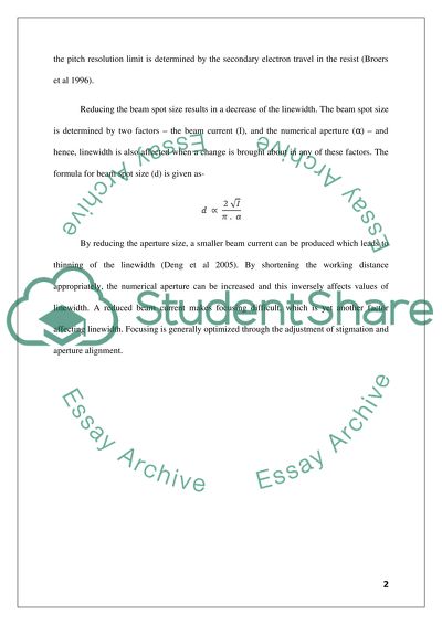
Reducing the beam spot size results in a decrease of the linewidth. The beam spot size is determined by two factors - the beam current (I), and the numerical aperture () - and hence, linewidth is also affected when a change is brought about in any of these factors. The formula for beam spot size (d) is given as- By reducing the aperture size, a smaller beam current can be produced which leads to thinning of the linewidth (Deng et al 2005). By shortening the working distance appropriately, the numerical aperture can be increased and this inversely affects values of linewidth.

A reduced beam current makes focusing difficult, which is yet another factor affecting linewidth. Focusing is generally optimized through the adjustment of stigmation and aperture alignment.Works CitedElectron Beam Lithography [online]. Silicon Far East, 2004. Available from: [Accessed 21/04/09]Rai-Choudhury, P. (ed.) Handbook of Microlithography, Micromachining and Microfabrication. Cornell NanoScale Science & Technology Facility, Ithaca.Deng, J. D. et al. (2005). E-Beam Lithography with 10nmlinewidth on PMMA.

CNS Cleanroom User Meeting.Broers, A. N. et al. (1996). Electron beam lithography - Resolution limits. Microelectronic Engineering, (32), pp. 131-142.Polymethylmethacrylate [online]. The Free Dictionary. Available from: [Accessed 21/04/09]

Read More
Cite this document
  • APA
  • MLA
  • CHICAGO
(“Electron Beam Lithography Lab Report Example | Topics and Well Written Essays - 500 words”, n.d.)
Electron Beam Lithography Lab Report Example | Topics and Well Written Essays - 500 words. Retrieved from https://studentshare.org/miscellaneous/1529533-electron-beam-lithography
(Electron Beam Lithography Lab Report Example | Topics and Well Written Essays - 500 Words)
Electron Beam Lithography Lab Report Example | Topics and Well Written Essays - 500 Words. https://studentshare.org/miscellaneous/1529533-electron-beam-lithography.
“Electron Beam Lithography Lab Report Example | Topics and Well Written Essays - 500 Words”, n.d. https://studentshare.org/miscellaneous/1529533-electron-beam-lithography.
  • Cited: 0 times

CHECK THESE SAMPLES OF Electron Beam Lithography

The Fabrication Of Bipolar Junction Transistors By Diffusion Planar Process

The fabrication of Bipolar Junction Transistors (B.... .... .... by the Diffused Planar Process is the objective of this report.... The diffused planar process is self-explanatory in itself by the name.... “The diffusion method for manufacturing junction transistors, pioneered by C.... A.... Lee at Bell Labs, uses a vapour of the impurity atoms surrounding the semiconductor material as it is heated....
9 Pages (2250 words) Lab Report

Semiconductor manufacturing research paper

This is so because these alter the anodization current and the electron concentration.... 1.... Plasma/remote plasma oxidation of silicon Remote Plasma-assisted oxidation of Silicon is primarily a process of low temperature, about 300oC for formation of device-quality interfaces on silicon....
12 Pages (3000 words) Research Paper

Current and Future Trends in Micro Electro Mechanical Systems

LIGA is a technology which creates small, but relatively high aspect ratio devices using x-ray lithography [9].... MEMS or Micro Electro-Mechanical Systems, also referred to as micro-machines is an emerging technology, which has had a phenomenal growth in the past decade.... This technology is well suited to producing a class of micro-machined sensors and actuators that combines signal processing and communications on a single silicon chip or contained within the same package....
6 Pages (1500 words) Case Study

New Product Packaging

In the research paper “New Product Packaging” the author analyzes the main objectives of the packaging, which include the cost of the carton, the time required for packaging, protection of the product, retail stores requirements, and branding information.... hellip; The writer insists that creative packaging will make the product successful, hence, our objective first will be creating a very attractive packaging that will emotionally connect with the consumers....
4 Pages (1000 words) Research Paper

Metal-Insulator-Semiconductor Contacts, and Spin Coating

V is the energy level in the valence band, EC is the energy level in the conduction band, EF is the Fermi level, χs is the electron affinity for the semiconductor, e (or q) is the carrier charge, φB is the Schottky barrier height.... The barrier height is the difference between the metal work function and the semiconductor electron affinity:For an n-type semiconductor, it means that the work function of the metal is similar or lower than the difference between the energy at vacuum level and the lower energy level of the conduction band and the energy bands are bent downwards (Rhoderick, 1982)....
12 Pages (3000 words) Assignment

Microelectronics and Two Major Infrastructures: Photolithography and Particle Beam Lithography

But to make the use of the infrastructure possible, Savile (2008) advocates the use of two major methods, which are photolithography and particle beam lithography.... hellip; Through conventional lithography, microelectronics has come out with two major infrastructures that are generally accepted in literature for patterning nanoscale features....
16 Pages (4000 words) Research Paper

Aspects of Technology Update

The technology of flexible electronic paper display was developed by Hewlett-Packard in collaboration with Arizona State University and uses a manufacturing process that was invented by HP Labs known as Self-Aligned Imprint lithography, abbreviated as SAIL.... This coursework "Aspects of Technology Update" describes apps and their role....
7 Pages (1750 words) Coursework

Enhancing Stretchability of Flexible Electronics

The process is similar to lithography printing.... A permanent 2-micrometer line and dotted gold patterns were fabricated through the lift-off process and UV lithography.... The process is similar to lithography printing.... … The paper “Enhancing Stretchability of Flexible Electronics”  is a thrilling variant of research paper on engineering and construction....
7 Pages (1750 words) Research Paper
sponsored ads
We use cookies to create the best experience for you. Keep on browsing if you are OK with that, or find out how to manage cookies.
Contact Us